Thick Copper PCB
Features
- Both double-sided and multi-layer PCB compatible.
- Can be applied in automotive and power module.
- Our support begins from development stage to suite the needs of customers quickly.
Our factory manufactures 105μm thickness.
Standard Specification
| Item | PCB Specifications | |||
|---|---|---|---|---|
| Double-sided | 4 Layers | |||
| Thickness [mm] | 1.0–1.6 | 1.6 | ||
| Cu Thickness [μm] | Base Cu Foil Thickness | Outer Layer | 105/175 | 18/35/70/105 |
| Inner Layer | - | 105/175 | ||
| Final Cu Thickness |
18 | - | 38–55 | |
| 35 | - | 55–72 | ||
| 70 | - | 90–107 | ||
| 105 | 125–142/150–167 | 125–142/150–167 | ||
| 175 | 195–225 | - | ||
| Min. Drill Diameter [mm] | φ0.65 | |||
| Min. Land Diameter [mm] | Outer Layer | Drill Diameter+250 | Drill Diameter+250 | |
| Inner Layer | - | Drill Diameter+350 | ||
| Min. L/S [μm] | Outer Layer | 18 | - | 125/125 |
| 35 | - | 150/150 | ||
| 70 | - | 300/300 | ||
| 105 | 300/400 | 300/400 | ||
| 175 | 300/500 | - | ||
| Inner Layer | 35 | - | 100/100 | |
| 70 | - | 150/150 | ||
| 105 | - | 200/200 | ||
| Solder Resist Ink (Alkali Development) | Green | |||
| Surface Treatment | Pb-free Solder Level / OSP / Gold Plating (Electro / Electroless) | |||
| Cross Section | Outer Layer Copper Foil Thickness: 175μm 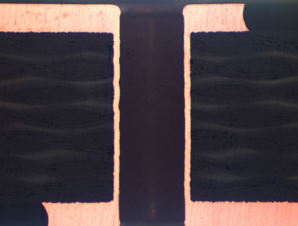 |
Inner Layer Copper Foil Thickness: 105μm 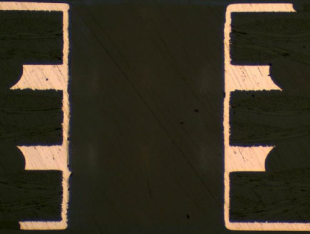 |
||
Properties
| Category | Test Condition | Result | |
|---|---|---|---|
| Mechanical Test |
1. Peel Strength | Pretreatment(260+5-0[°C]/3–4[sec]) : Peel test |
Copper foil 18 [μm] material: more than 11[N/cm] Copper foil 35 [μm] material: more than 15[N/cm] |
| 2. Coating Hardness | JIS C 5012 : Pencil scratch harness test |
Alkali development type: More than 4H | |
| 3. Coating Hardness | Pretreatment( 260+5-0[°C]/3–4[sec]) : Grid scratch test |
100 last out of 100 | |
| 4. Solder Heat Resistance | Pretreatment( 40[°C]/90[%]/96[hr]) : Solder Floating Method( 260+5-0[°C]/3–4[sec]) |
No floating of copper or delamination or inflation | |
| Electrical Test |
5. Withstand Voltage | Applied voltage(100/500/1000[V]/1[min]) : Between the same side Min. space 0.10–0.13[mm] Test voltage 100[V] Min. space 0.15[mm] More than Test voltage 500[V] : Between the opposite side Layer distance 0.80[mm] Less Than Test voltage 500[V] 0.80[mm] More than Test voltage 1000[V] |
No Mechanical damage, flash over, spark over, breakdown |
| 6. Insulation | Applied voltage(100/500[V]/1[min])→Insulation resistance : Between the same side Min. space 0.10–0.13[mm] Test voltage 100[V] Min. space 0.15[mm] More Than Test voltage 500[V] : Between the opposite side Layer distance 0.80[mm] Less Than Test voltage 100[V] 0.80[mm] More Than Test voltage 500[V] |
More than 1GΩ | |
| Environmental Test |
7. Migration Resistance | Pretreatment( 85[°C]/85[%]/250[hr]) Applied voltage(50[V]) : Insulation resistance, visual inspection |
More than 1GΩ, no dendrite |
| 8. Thermal Shock Test | 260+5/0[°C]/10[sec] : 20±5[°C]/20[sec] 50[Cycle] |
Change rate of conductor resistivity less than 10 [%] | |
Above spec can be changed without notice.